A Lean Fabless Semiconductor Startup Model
Introduction
There is currently a general consensus among industry analysts, investors, and company executives that leading edge digital chip development projects costs $30-$100M to develop. This negative view of chip development costs has led to severely decimated levels of VC investments and has even led to certain companies scrapping whole products lines.[1] Today’s chips have a bigger impact on the world’s economy than ever and reduced investments in chip product development will eventually have a very negative impact on the economy. China for one has realized this and is pouring billions of dollars into their local semiconductor economy.[2] This article will go through some of the reported data and show that present assumptions regarding chip development costs are very much exaggerated and that it is possible to design state of the art chips at a fraction of the cost previously reported.
Why is Chip Development so Expensive?
Chip development has never been cheap and there is no question that it’s getting more expensive. The million dollar question is: “how much more expensive?” The consensus among industry pundits is that there is no way to do a leading edge chip with less than $30-$100M.[3-4] Let’s take a look at some of the most common arguments for the “exponential” increase in chip development costs.
“Mask costs are increasing exponentially!”
It used to be that you could design a product with production mask costs in the range of $100K. Today, production mask costs at leading nodes can cost $1-2M. This has the effect of increasing the minimum market size that is practical to address with a leading edge chip design. Still, given a decent size market or high chip selling prices, mask costs are certainly not show stoppers and don’t explain the $100M price tag.
“EDA tools are getting really expensive!”
While EDA tools are certainly not cheap, aggressive volume purchasing agreements, increased feature integration and increased efficiency in the tools have made today’s tools far more cost effective than those of ten years ago. Today many leading chips can be taped out using vanilla flows derived from reference scripts provided by the EDA vendor. Thus, per transistor and per project, the cost of EDA tools has actually gone down in the last ten years.
“Deep submicron design is really hard!”
Chip design is certainly getting more difficult as we move to finer process geometries. At 0.35um and above, life was simple. Gates were slow, wires were fast, and there was virtually no leakage to speak of. The only problem was that chips were slow, power hungry, and big! Since then, the design constraints and difficulties have been piling on with every process node. In order of introduction designers had to learn and deal with: wire delays, voltage drops, signal integrity, leakage, process engineering effects like stress, and most recently on chip variability and an explosion in the number and complexity of device design rules. The introduction of each one of these effects was painful, but within one process generation, the EDA industry always seemed to find automated methods of dealing with them, thus keeping engineering team growth to a minimum. Deep submicron chip design is definitely not for hobbyists, but for a small expert team equipped with state of the art tools, it is today possible to accomplish in weeks what used to take a generously sized team 6-9 months. [5]
“Chips are getting incredibly complex!”
Bingo! The simple reason for the explosive growth in chip design costs is that design complexities are growing exponentially thanks to Moore’s Law. At leading edge nodes it is now possible to integrate complete multi-billion transistor computer systems on a single chip. The more complicated the system, the more complicated the chip. Complicated SOCs are indeed very expensive to develop and there are few if any examples of complete products that have cost less than $10M from start to finish. An ASIC on the other hand tends to solve a very specific problem and be key part of a larger system. The limited generality of ASICs can lead to much higher performance levels and generally results in reduced complexity and development. For a great discussion of the relationship between project complexity, team sizes, and project costs, I highly recommend reading “The Mythical Man-Month”, by computer legend Fred Brooks. Unfortunately, there aren’t a lot of short cuts for saving costs when projects are complex and need to be completed in a short time. Note that complexity drives up development costs of any project, regardless of the underlying implementation fabric. As many designers are discovering, large FPGAs have all of the complexity problems of large SOC design, minus the long turnaround time and costs of manufacturing.
The Status-Quo Fabless Semi Startup Model
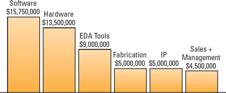
Figure 1 shows the typical costs of reaching production for a state of the art SOC for a fabless semiconductor company. The data is based on personal experiences and numerous informal interviews with executives at chip startup companies who spent up to $50M without reaching break-even.
Figure 1: Typical SOC Costs
(Assumptions: 3 years from start to break even for product, $150k/engineer, 75 Person Company)
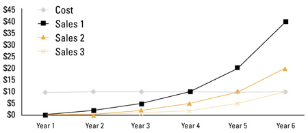
Clearly, despite the large EDA tool component and mask building costs, by far the largest project costs is engineering. Figure 2 illustrates the biggest issue with the large burn rate business model shown above. It’s incredibly sensitive to delays in “time to money”, whether the delays are due to design slippage or market materializing late. The figure shows three potential sales models with different degrees of eternal optimism built in. Anyone involved with semiconductor product sales knows that it’s incredibly hard to get toe $10M in profits for a chip product per year. The good news is that if you do, the potential upside is huge. The downside for startup companies without deep pockets is that if the company runs out of money before profitability is reached it is again at the mercy of investors and/or macro-economic conditions. Many companies on the verge of greatness went out of business in 2008 because they ran out of money at the wrong time. Since time to sales carries the most amount of uncertainty, reducing the R&D expenses though the initial sales period can significantly increase the likelihood of success given a fixed investment size.
Figure 2: High Burn Rate Semiconductor Business Model
Choose your Market
As we discussed, the biggest contributor to semiconductor development cost is design complexity. The easiest way to reduce design complexity is by picking the right market. The market will drive feature sets and chip selling prices. By far the most extreme example is the SOC application processor in a cellular phone. Half a billion transistors, every I/O interface one can think of, and yet the average selling price is often less than large latte at your local café. This is not a good space for a startup, as the total investment in software and hardware could actually reach $1B at the end of the day!
Markets that are not quite as cost and space sensitive have a huge advantage in terms of development costs savings, because they allow companies to leverage existing chips in the market to make chip set solutions that satisfy the system requirements. For example, it is possible to buy off the shelf FPGAs and/or microcontrollers for $1-10 that will give a system a complete host computer and every connectivity standard in the book. High end I/O IP such as PCIe, DDR, USB, and Ethernet are very expensive to design into SOCs and choosing all of them on a single chip adds a lot of cost and risk to a project. It’s not just the purchasing costs, it’s also the integration, validation, and testing costs in addition to the sticker price. The trend towards inexpensive mid end FPGAs is especially encouraging, as it allows the fabless startup company to go after a large number of markets with a single chip platform. Software development costs also have a huge impact on product development. Some markets demand that the chip vendors develop the whole software stack and give it away for pennies. Unless you are designing a system solution, and get a good return on investment always focus on “teaching your customer to fish rather than giving him the fish for free”.
Further Costs Cutting Measures
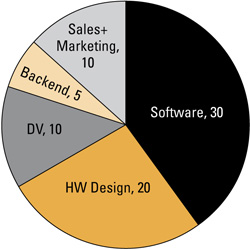
Figure 3 shows the man-power breakdown for a typical modern fabless semiconductor startup company. On average the SOC startup team seems to ramp up to approximately 75 engineers quickly and stay at that team size until eventually ramping up towards an exit or going out of business.
Figure 3: SOC Design Team Composition
If we turn the fabless semiconductor business model on its head and ask the question: “What could be done about spending if we are willing to give up time and some down the road profits instead of trying to minimize time to product at all costs?” Let’s go through each one of the expense categories, and look at some things that could be done to reduce costs.
- Software: Many chips today are sold with a complete accompanying software stack. The big problem is that the chip vendors rarely get properly compensated properly for the software by the OEMs. The question posed is often: “Why should we pay for the software. We can’t use your chip without it and we really aren’t interested in learning the inner workings of your chip to be able to program it ourselves”. Two potential solutions to reducing software R&D include: 1.) Design your architecture so that you can leverage existing open source software packages (e.g. make it ANSI-C programmable in the case of processors) 2.) Make the chip attractive and easy enough to use, that the customer can effectively do the programming himself.
- Hardware: Quoting the slogan of the green movement. “Reduce, Reuse, and Recycle”. The way to reduce hardware development costs is by 1.) Reducing the feature set that needs to be implemented and by 2.) Maximizing the reuse of validated blocks [6] 3.) Recycling all the great chip ideas of the last 70 years (no Not-Invented-Here nonsense allowed). Reuse is one of the key competitive advantages in the chip industry. An SOC company that does not embrace reuse as a basic design imperative will not be profitable in the long run, because they will miss market windows and have R&D costs that are far too high.
- Design Verification: Reduced design complexity again comes to the rescue and the key here is really to not to be “too clever”. The prevailing method of chip development usually involves an experienced system architect writing a set of specifications that are then given to a team to design and verify. Without close interaction from day one between the architects and the complete design team, this almost certainly causes expensive problems downstream. In the words of Richie Kernigan. “Debugging is twice as hard as writing the code in the first place. Therefore, if you write the code as cleverly as possible, you are, by definition, not smart enough to debug it.” Designing architectures that can easily be verified with a small team is an art form that requires very tight integration between the architecture, design, and verification teams.
- Backend: There is a rich ecosystem of support companies that can take over as much or as little of the chip business the client requests. Opportunities for out-sourcing include: manufacturing (a must!), RTL design, synthesis, verification, package design, board design, testing, and logistics. If your core competency is chip design and computer architecture, then outsourcing software, board design, sales, marketing, logistics makes sense. If your core competency is system architecture, outsourcing a large part of the chip design makes sense, but make sure you find the right implementation team.
- Sales/Marketing: Selling chips with power-point presentations has never worked and really just wastes money and burns out the sales and marketing team. The bigger the claim of the chip the smaller the chance that the customer will do anything before he gets his hands on a board level development system. If you have a low R&D burn rate, you can be less aggressive with the pre-product sales and marketing effort and subsequently waste less money.
A Case Study
Adapteva has completed four generations of low power multicore chips and have reached product release status. We used many of the techniques discussed to reach break–even with less than $2M of total investment.
- Market Choice: We chose the military embedded computing and high performance computing as initial markets mainly because it allowed us to reduce development costs. These markets already knew how to do parallel programming so they didn’t require a big support infrastructure, didn’t require extensive software stacks, and were fairly insensitive to chip costs. In terms of software and hardware development, this allowed us to reduce the combined software and hardware design team from 30+ engineers to 3 engineers! Because of the high chip selling prices, it also allowed us to ramp up chip production using multi-project shuttles, while still selling devices for a profit. The multi-project shuttle model could never work for consumer type devices, with selling prices of a few dollars per chip.
- Slow It Down: We traded market penetration for money by: 1.) Staffing up very slowly and only when we absolutely had to 2.) Using multi-project wafers extensively to delay the million dollar mask costs until we have firm large orders on the books and the product was “perfect”. Ideas take time to gel and the size of the team has very little impact on progress in the beginning. Staffing up too quickly before the infrastructure is in place will waste money and can even force bad design decisions. Sales ramps are always slower than forecasted, and in our case we saw very little negative impact of our low burn rate.
- Reuse: This was one of the fundamental design principles for our company. At the first level we reused/leverage existing chips in the market (FPGAs and ASIPs) by deciding not to take on the whole system definition for the chip, and suggesting instead a chip set solution for the customer. Inside the chip, we leveraged off the shelf physical IP and reused every line of internally developed RTL code as many times as possible.
- Partnerships: We were lucky to find great tier-one development partners for manufacturing, development tools, and board development. Working with the best in the business allowed us focus on our core competency and off-load any work that we didn’t have expertise in.
Conclusion
Yes, it is possible to spend $100M (or even $1B) on chip development, but it’s also possible to spend as little as $2M to reach profitability as a fabless semiconductor company.
Andreas Olofsson is the founder of Adapteva and the creator of the Epiphany architecture and Parallella open source computing project. Follow Andreas on Twitter.


